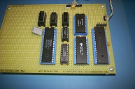
Version 2
Version 2 adds a little more glue logic to allow the PIC to control the 8085 like an Altair front panel. It can perform the run/stop, single step, deposit, deposit next, examine and examine next functions.
Theory of Operation
The core system consists of the CPU, Memory, and UART. The PIC microcontroller controls the CPU and memory in the same way as the original Altair front panel by using the READY line. The READY line was intended to deal with slow memories or IO devices. Activating the READY line causes the CPU to insert wait cycles. If this is done during a memory read operation, the address bus will contain the memory address supplied by the CPU. If it is done during an instruction fetch cycle, instructions can be jammed on to the data bus. The PIC can jam a JMP instruction on to the data bus to set the CPU program counter to a new address. It can also jam a NOP instruction to go to the next address. By pulsing the memory write line, the PIC can write to memory at the current address. Using this method, the PIC performs the Run, Stop, Examine, Examine Next, Deposit, Deposit Next., and Single Step functions.Schematic
Note the schematic does not show all the power supply and ground connections to the chips or the bypass capacitors. Although the address lines A8 - A15 are still shown connected to the PIC, they are not used and can be removed.CPU
The 8085 runs at 3 MHz clock frequency with a 6 MHz crystal. The READY line is used to force the CPU to execute wait cycles while the PIC controls the data bus.Address Latch
The lower 8 bits of the address is latched off of the data bus with a 74LS373. The latch is clocked at the beginning of each machine cycle by the 8085 ALE line.RUN STOP STEP Flip-Flops
The 74LS74 D flip-flops are used to synchronize the READY line with the 8085 memory read cycle. If the RUN line is low, the READY line stays high and the 8085 runs normally. When the RUN line goes high, the READY line will go low at the next rising clock edge after ALE goes high. This causes the 8085 to enter wait cycles while presenting a valid address on the address bus and waiting for valid data on the data bus. If the STEP line goes low to high, READY will go high and the 8085 will finish executing the machine cycle and stop at next cycle when ALE goes high again.Memory
32K bytes of static RAM is provided by a CY62256. The memory can be accessed by either the 8085 or the PIC. The read input is driven by RAM RD which goes low when RD from the 8085 goes low if RAM RD DIS is not high. The PIC raises RAM RD DIS to disable the RAM and insert data onto the data bus. The write input is driven by RAM WR which goes low if either WR from the 8085 or RAMWROUT from the PIC goes low. The RAM is enabled by RAMCE when the address is in the lower 32KB of the address space and the current CPU cycle is a memory access (not an IO cycle).UART
The 6850 UART is only accessed by the 8085. UCLK is the baud rate clock which is generated by the PIC. The 6850 bus interface is clocked by the E line which is driven by UE. UE is asserted whenever RD or WR go low. The 8085 status signal S1 provides an early R/W signal that is stable when E is pulsed. The UART is intended to be mapped to IO addresses 020 and 021 (octal). Actually only address bits A0, A4 and A7 are decoded, so the UART will respond to any addresses 0XX1XXX0 and 0XX1XXX1. RxData and TxData are 5V RS232 lines and must be converted by a level shifter like a MAX232 to connect to a true RS232 terminal or a PC serial COM port.PIC
The PIC18F320 microcontroller performs several functions. It runs off it's internal oscillator at 8 MHz (2 MIPs).- It uses a PWM peripheral to generate the baud rate clock for the UART, output UCLK. This clock is 16 times the baud rate. For 9600 baud, it is 153.6 kHz.
- It is connected to the data bus and can write to RAM or jam instructions onto the bus for the 8085 to execute. It connects to the data bus through the PIC's PSP (Parallel Slave Port). The chip select line for the PSP is driven by MCUCS, which it can force low with the CSOUT output, causing the 8085 RD and WR to access the PSP.
- It controls the 8085 READY line through the RUN STOP STEP flip-flops.
- It controls the 8085 RESET line. When RESET is released, the 8085 starts running at address 0.
- It mimics the Altair sense switches. This PIC has a PSP (Parallel Slave Port) peripheral which is an 8 bit parallel port with asynchronous RD and WR and CS inputs. The MCUCS line is decoded when address bit 7 and an IO operation is taking place. If the 8085 reads IO address 377 octal (the location of the sense switches), it will read the PSP. The PIC pre-loads the PSP with the sense switches setting. This function is necessary because Altair BASIC reads the sense switches to determine which UART driver code to use. Since only address bit A7 is decoded, any access to IO addresses 1XXXXXXX will access the sense switches register.
