Version 3
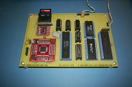
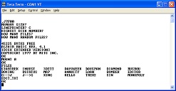
Version 3 adds a floppy disk emulator using an SD card for storage. The hardware emulator is register-compatible with the 88-DCDD Altair Floppy Disk System. This allows all of MITS disk software (disk BASICs and Altair DOS) to run unmodified. The floppy data is stored on the SD card using the FAT32 file system so disk images can be easily transferred to other computer systems. The disk images are stored as files which are straight binary images of the floppies. This is the same format as the Altair32 emulator so the images provided in the emulator can be used directly and exchanged between the emulator and the Mini-Altair. With the disk emulator, the Mini-Altair connected to a dumb terminal becomes a complete stand-alone computer system without the need to ever connect to another computer in order to operate.
Theory of Operation
The 88-DCDD
The 88-DCDD floppy disk controller is documented in the Altair Floppy Disk System manual. The interface is very basic and uses only three IO ports. The hardware for the disk interface emulator is consequently very simple. A PIC microcontroller is used that has a PMP (Parallel Master Port) interface. The parallel master port has an addressable slave mode that provides 4 parallel ports that are addressable with 2 address bits. It can be configured to use RD, WR and CS lines to interface with a microprocessor. The PIC also has an SPI (Serial Peripheral Interface) that can be used to interface with the SD card.Supply Voltage Constraints
The 8085 uses a 5V power supply and 5V TTL logic levels. The SD card uses 3.3V power supply and TTL levels. All of the PICs that have the PMP interface use 3.3V power supplies. Typically some of the PIC interface pins are 5V tolerant inputs. This means they can be directly connected to 5V TTL signals and function without damage. 3.3V TTL output levels are compatible with 5V TTL input levels, so they can also be directly connected and function without damage.Schematic
Note the schematic does not show all the power supply and ground connections to the chips or all the bypass capacitors.PIC
The PIC 24FJ128GA106 was chosen because it has a Parallel Master Port (PMP) which can be configured in an addressable slave mode to provide an interface to the 8085 data and address bus. The 8 data bits for the PMP and the RD, WR, and CS lines for the PMP are all 5V tolerant so they can be directly connected to the 8085 bus. Only the two address bit inputs are not 5V tolerant and require a level shifter. The CS line is active whenever there is an IO operation and the IO address is 0XXX1XXX. The PIC can be directly connected to and SD card and the PIC's SPI peripheral can be used to interface with the SD card. Microchip, the manufacturer of the PIC, provides a firmware library to use the SD card as a FAT32 formatted solid state disk drive. The PIC internal oscillator is used at 32MHz for 16MIPs operation.SD Card
The SD card is used in SPI mode and requires only two data lines, a clock line, and 3.3V DC power. The SD card is connected directly to the PIC. The SPI lines can be connected to any of the pins that are selectable with the Peripheral Pin Select feature of the PIC. The CS input to the SD card and CD and WP outputs are connected to PIC IO port pins.3.3V - 5V Buffer
The 74LVC125 is used as a 5V to 3.3V level shifter for the two address bits A0 and A1 that are connected from the 8085 address bus to the PIC.Regulator
The LM3940 is used to provide a regulated 3.3V for the PIC, the SD card and the buffer. It is supplied by the 5V Vcc.Firmware
The PIC firmware is written in C for the Microchip C30 compiler. A free version of the compiler is available. It utilizes Microchip's Memory Disk Drive File System library. "FSIO.h" references the MDDFS library. "PPS.h" references the peripheral pin select functions provided with the compiler. <ports.h> references the port functions provided with the compiler.PMDRead1bits are the bits for reading the IO ports 11 and 10 (octal). The PIC24 is a sixteen bit processor, so its IO ports are two bytes wide. PMDWrite1bits are the bits for writing to ports 11 and 10 (octal). Port 12 (octal) is the disk controller data port.
The firmware is interrupt driven. The main function starts by initializing pFile[], which is an array of file handles, one for each drive. The file named "DISKx.DSK", where x is the hex number of the drive, is opened for each drive. Track[] is an array of the current track for each drive. The PIC clock is set to 32MHz for 16MIPs operation. The peripheral pin select is set up for the SPI port. Pullups are set up for the CD (Card Detect) and WP (Write Protect) inputs from the SD card. PMDOUT1 is the parallel master port lower two bytes connected to the 8085 IO ports 11 and 10 (octal). PMDOUT2 is the PMP upper two bytes connected to IO port 13 and 12. Port 13 is not used.
The interrupt handler is triggered whenever the PMP ports are read or written by the 8085. Timing is critical here, so the interrupt routine is intended to complete as soon as possible.
The main loop handles tasks that require more time such as reading and writing to the SD card. Handshaking with the interrupt routine and the 8085 is accomplished by manipulating the status bits of PMDRead1bits and the flags NeedToRead, NeedToWrite and NewSector.
Timing Constraints
The various disk drive operations take time to complete, and the MITS software takes these times into account: After issuing the head load command, the head load status bit is queried in a wait loop until head is loaded. After issuing a step in or step out command, the move complete bit is queried in a wait loop until move is complete. The sector true bit is queried in a wait loop to wait for the beginning of a sector to move into position under the head. The read data available bit is queried in a wait loop before reading a byte from the controller and writing to a memory buffer. Since the data is available once every 32 micro-seconds, there isn't time for the 8080A CPU to check the read data available bit every time, so it reads two bytes at a time. The instruction cycles are carefully calibrated so that the two reads are slightly longer than 32 micro-seconds apart. For this design, using an 8085 running at 3MHz, the time is reduced to roughly 20 micro-seconds. Writing is similar to reading, except the write data ready bit is queried.This puts constraints on the PIC firmware timing. For example, when reading from the data port, the next data byte must be ready within 20 microseconds from the previous read. Operations that take a relatively long time, like reading and writing from the SD card, cannot block responses to reads and writes by the CPU to the data ports. Use of the PMP, which has one byte read and write buffers on each port, and a fast interrupt routine with careful use of the status bits are used to prevent this type of conflict.

